Pascal GPU memory and cache hierarchy
Memory access efficiency allows fully utilizing the computational power of graphics processing units (GPUs). However, many GPU vendors like NVIDIA kept the GPU memory hierarchy as a secret. Therefore it becomes hard to measure GPUs performance and sets barriers to understand memory access patterns, which is a key component to improve program’s performance.
We introduce a novel fine-grained micro-benchmark approach and apply to the Pascal generation. Turing architecture might have different results, but the method we used here can be applied as well with slight modification. The method we use in this guide is inspired by the research paper: Dissecting GPU Memory Hierarchy through Microbenchmarking. Here we will explain how P-Chase works and walk through a small example.
Memory Hierarchy Overview
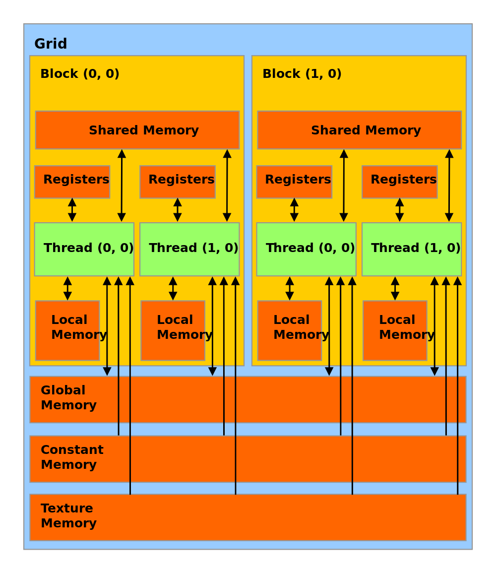
GPU memory hierarchy is different compared to CPU memory hierarchy. Using the terminologies of CUDA, GPU memory space can be categorized in these groups: register, constant memory, shared memory, texture memory, local memory, and global memory. Each different memory space have its own properties. Since we are interested the cache systems, here is a picture demonstrating the memory hierarchy of a NVIDIA GPU:
The characteristics of each memory space can be found in NVIDIA CUDA C Programming Guide . Here we will focus on some target memory space we are interested in. The paper lists some properties of our target memory space:
| Memory | Type | Cached | Scope |
|---|---|---|---|
| Global | R/W | Yes | All Threads |
| Shared | R/W | N/A | Thread Blocks |
| Texture | R | Yes | All Threads |
Even though the paper targets Fermi, Kepler and Maxwell generations of GPU, the properties of the table still holds for Pascal GPU and possibly Turing as well. The cached global/texture memory uses a two-level caching system. The L1 cache is located in each stream multiprocessor (SM), while the L2 cache is off-chip and shared among all SMs. It is unified for instruction, data and page table access. According to CUDA documentation, like Maxwell, Pascal combines the functionality of the L1 and texture caches into a unified L1/Texture cache which acts as a coalescing buffer for memory accesses, gathering up the data requested by the threads of a warp prior to delivery of that data to the warp. This function previously was served by the separate L1 cache in Fermi and Kepler. Page table is used by GPU to map virtual addresses to physical addresses, and is usually stored in the global memory. The page table is cached in TLB to reduce memory access latency. Once a thread cannot find the page entry in the TLB, it would access the global memory to search in the page table, which introduced significant memory access latency. The GPU-specific shared memory is located in the SMs. On the Fermi and Kepler devices, it shares memory space with the L1 data cache. On Maxwell and Pascal devices, it has a dedicated space, since the functionality of the L1 and texture caches have been merged. One thing to note here is that shared memory is accessed by the thread blocks. Thread-blocks remain limited to 48 KB of shared memory in Pascal. Therefore, NVIDIA recommends that applications use at most 32 KB of shared memory in any one thread block. This would, for example, allow at least two thread blocks to fit per GP100 SM, or 3 thread blocks per GP104 SM.
However, we should be careful that by default, GP100 caches global loads in the L1/Texture cache. In contrast, GP104 follows Kepler and Maxwell in caching global loads in L2 only, unless using the LDG read-only data cache mechanism introduced in Kepler. As with previous architectures, GP104 allows the developer to opt-in to caching all global loads in the unified L1/Texture cache by passing the -Xptxas -dlcm=ca flag to nvcc at compile time. Even though both GP100 and GP104 belongs to Pascal family, we only focus on GP100 here because that’s the GPU we use. Another thing to notice is that unlike Maxwell but similar to Kepler, Pascal caches thread-local memory in the L1 cache. This can mitigate the cost of register spills compared to Maxwell. To illustrate our point, we checked both cudaDevAttrGlobalL1CacheSupported and cudaDevAttrLocalL1CacheSupported on Tesla P100 and GTX 1080 and find both attributes to be 1.
In addition to the L2 data cache, global memory data that is read-only for the entire lifetime of a kernel can be cached in the read-only data cache with a compute capability of 3.5 or above. We will also explore the size of this read-only cache using __ldg() intrinsic.
P-Chase
Most existing GPU microbenchmark studies on cache architecture assume a classical set-associative cache model with the least recently used (LRU) replacement policy, the same as the conventional CPU cache. So here we will use this assumption and proceed with our experiments. Here are some notations we will use throughout this post.
| Notation | Description | Notation | Description |
|---|---|---|---|
| C | Cache Size | N | array size |
| b | cache line size | s | stride size |
| a | cache associativity | k | iterations |
| T | number of cache set | r | cache miss rate |
Under our assumptions, data is loaded from main memory to lower cache in the basic unit of a cache line. The number of words in a cache line is referred to as the line size (b). For the LRU set-associative cache, the cache memory is divided into T cache sets, each of which consists of \(a\) cache lines. It is essential to have these three assumptions using this kind of cache model:
Assumption 1 All cache sets have the same size. The cache parameter should satisfy \(T \cdot a \cdot b = C\).
Assumption 2 In the memory address, the bits representing the cache set are immediately followed by the bits representing the offset.
Assumption 3 Cache replacement policy should be LRU.
We will later see why these assumptions are essential as we proceed with the experiment. We won’t go through how P-Chase work exactly. To find more information, this paper does a good job illustrating how P-Chase work. The takeaway is, we need to brute force an array with one element more than a cache can hold so that cache miss will start to occur periodically whereas such array with less or equal elements to the cache capacity will always result in cache hit and thus no access overhead will be introduced after all data is loaded into the cache. This is the algorithm the paper proposed and we will use it to do the experiment:
__global__ void KernelFunction ( . . . ) {
    //declare shared memory space
    __shared__ unsigned int s tvalue [ ] ;
    __shared__ unsigned int s index [ ] ;
    preheat the data ; // implementation varies
    for (it = 0; it < iter ; it++) {
        start_time=clock();
        j = my_array[j];
        //store the array index

        // This following line is essential because due to
        // instruction-level parallelism (ILP), function clock() may
        // overlap with its previous instruction and even return before
        // the previous instruction finishes. For example,
        // end_time=clock() can return before j = my_array[j] returns.
        // adding s_index [it]= j since it have data dependency on the
        // previous line. Thus the memory access will be over before
        // end_time=clock() started.
        s_index [it]= j;
        end_time=clock();
        //store the access latency
        s_tvalue[it]= end_time−start_time ;
    }
}
The steps is the same as the paper proposes, so here we show the paper’s method:
Determine cache size C . We set s to 1. We then initialize N with a small value and increase it gradually until the first cache miss appears. C equals the maximum N where all memory accesses are cache hits.
Determine cache line size b. We set s to 1. We begin with N = C + 1 and increase N gradually again. When N < C + b + 1, the numbers of cache misses are close. When N is increased to C + b + 1, there is a sudden increase on the number of cache misses, despite that we only increase N by 1. Accordingly we can find b. Based on the memory access patterns, we can also have a general idea on the cache replacement policy.
Determine number of cache sets T . We set s to b. We then start with N = C and increase N at the granularity of b. Every increment causes cache misses of a new cache set. When N > C + (T − 1)b, all cache sets are missed. We can then deduce T from cache miss patterns accordingly.
Determine cache replacement policy. As mentioned before, if the cache replacement policy is LRU, then the memory access process should be periodic and all the cache ways in the cache set are missed. If memory access process is aperiodic, then the replacement policy cannot be LRU. Under this circumstance, we set N = C + b, s = b with a considerable large k (k » N/s) so that we can traverse the array multiple times. All cache misses are from one cache set. Every cache miss is caused by its former cache replacement because we overflow the cache by only one cache line. We have the accessed data indices thus we can reproduce the full memory access process and find how the cache lines are updated.
Texture L1 Cache and Read-only Data Cache
When use the code with increased our own data preheat implementation because the texture L1 cache can potentially be greater than the shared memory. The original code uses the first iteration of the loop in the algorithm as a way to preheat data:
const int it =  6144 // texture L1 may hold more elements,
                     // So the first iteration may not cold
                     // hit all elements, some cold hits can
                     // be moved to the second iteration,
                     // causing confusion
for (int cnt=0; cnt < it; cnt++) {
    start=clock();
    j=tex1Dfetch(tex_ref, j);
    s_value[cnt] = j;
    end=clock();
    s_tvalue[cnt] = (end -start);
}
However, if texture L1 cache is greater than the shared memory allowed for each thread block, then some reads in the second loop will trigger cache misses. But such misses are in fact cold misses, not misses caused after the texture L1 cache is completely filled up. One solution is increase iteration to a much larger number so that the first iteration will always fill up the texture L1 cache. Note that if you move the data preheat out such as
for (int cnt=0; cnt < it; cnt++) {
        tmp=tex1Dfetch(tex_ref, tmp);
}
The compiler can optimize this whole step out and thus nothing actually gets executed.
After we run the modified code, the result shows that the we the cache missed starts when we set our array size to 6145, indicating the texture L1 cache can hold 6144 ints, which is equivalent to 24 kb. We also notice that each miss is followed by 7 consecutive hits. This means the cache line size is 8 words(b = 32 bytes). The structure of the L1 TLB is shown below, notice there are 192 lines in each set:
| Set1 | Set2 | Set3 | Set4 |
|---|---|---|---|
| 1-8 | 33-40 | 65-72 | 97-104 |
| 9-16 | 41-48 | … | … |
| 17-24 | 46-56 | … | … |
| 25-32 | 57-64 | 89-96 | 121-128 |
| 129-136 | |||
| … | … | … | … |
| 2969-2976 | 3001-3008 | 3033-3040 | 3065-3072 |
According to CUDA documentation, GK110 adds the ability for read-only data in global memory to be loaded through the same cache used by the texture pipeline via a standard pointer without the need to bind a texture beforehand and without the sizing limitations of standard textures. The read-only data cache is loaded by calling __ldg(const restricted * address). We modified the code used to test texture L1 cache. The basic logic remains the same. When the arrays size is set to 6144 integers no cache misses occur with stride set as 32 (s=32 bytes). As soon as we increased one more element in the array cache misses start occurring. This shows the read-only cache is 24kb. We then noticed that the misses occur in a group of either 4 or 8. We infer the cache line to be 32 bytes and the replacement policy is LRU, same as Maxwell. We we increase the array to include 6248 elements(6144+323+8, 6144 is the max capacity of the cache, 32 consecutive number in a set, 323 to cause cache miss in set1, set2, and set3, only need to include 8 more to cause cache miss in set4 since s=32bytes), no caches hits occur. Therefore, we infer the caches set number to be 4, each cache line is 32 bytes, and each set contains 192 cache lines, the same as the texture L1 cache. The memory mapping seems arbitrary because the hit and miss patterns didn’t follow that of the texture L1 cache.